Introduction to GALs and PALASM
In the mid 1970's "programmable logic device" (PLD)
chips started to appear that contained
reconfigurable
digital circuits.
Unlike 74xxx type
logic gates, which has a fixed function, a PLD
device has an undefined function at the time of manufacture. Before the PLD
could be used in a circuit it had to be "burned" or programmed, much like a ROM.
There were numerous early arrangements of this concept (ROAMs, PLA's etc.), but
a company called Monolithic Memories (MMI) introduced a breakthrough device in
1978, the Programmable Array Logic or PAL. These devices had arrays of
transistor cells arranged in a "fixed-OR, programmable-AND" plane that could be
used to implement "sum-of-products" binary logic equations for each of the
output pins in terms of the input pins. If required, they could also utilize
either synchronous or asynchronous internal feedback circuits from the outputs.
These "PALs" were soon second sourced by National Semiconductor, TI and AMD.
What really got the concept going was the simultaneous introduction of a
programming language to program/burn these PAL's. The language was called
PALASM. This language allowed the user to configure the
PAL essentially without any knowledge if it's internal workings.
MMI started with a 20 pin chip, AMD introduced a very flexible 24 pin chip the
so called 22V10 which proved very successful.
In 1985 Lattice Semiconductor significantly improved on the PAL concept by
making the chips electrically programmable (like EEPROMS). Until then all
PALs had a one time "burn" or programming function. If done wrong the PAL
was useless. These new electrically programmable chips were called GAL's. GALs
combine CMOS and electrically erasable (E2) floating gate technology
to yield a high-speed, low-power logic device, they essentially replaced PAL's
over time. In fact Lattice Semiconductor went on to acquired MMI.
Today Lattice and others have many more sophisticated and larger forms of these
chips, but in general the technology has evolved into FPGA devices.
However the simple 16V8 and 22V10 chips are still found in millions of
devices.
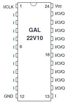
The GAL22V10
There are many types of GAL's available today. Very common are 16V8's,
20V8's and
22V10's. The first two digits refer to the total number of
programmable pins, the second the number of programmable inputs. Since
these chips are so inexpensive we will overkill, and concentrate on the 22V10.
If required we can just ignore any unused pins. Here is what the chip
looks like:-
A few points to keep in mind with this chip.
1. While any of the 22 pins can act as inputs or output pins, pins 1-11 and
13 can only behave as inputs.
2. If one or more outputs are to behave as "register" outputs, i.e. clocked or
latched, pin 1 is the clocking pin.
3. If one or more outputs are to utilize an OE control, pin 13 is the normal OE
pin.
4. Unconnected, all pins have an internal active pull-up connection.
5. The chip is capable of very high speed operation (166MHz), is TTL compatible,
able to sink 12 milli-amps per output pin.
6. The chip can not be programmed indefinitely.
Lattice quotes 100 erase/write cycles and data retention in excess of 20 years.
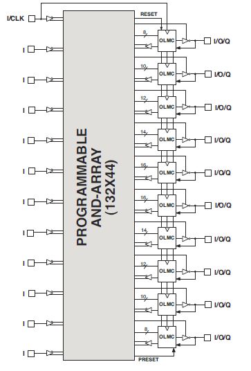
7. Note the number of possible input equation values that
use the OR statement for the output pins varies a
lot. They are as follows:-
Pins 23 & 14 = 8
(OR's)
Pins 22 & 15 = 10
(OR's)
Pins 21 & 16 = 12
(OR's)
Pins 20 & 17 = 14
(OR's)
Pins 18 & 19 = 16
(OR's)
Remember the number of product terms indicated for each pin
does not limit the AND statements, it limits only
the number of OR statements.
Be carefull not to overload these pins. Essentially for any one pin, there
should be less than 8 to 16 lines of code (if you had a "+" on each line).
This is not normally a problem but you should be aware of it.
For large PALASM equations you can use one output pin as a temporary placeholder
for a value used in a further pin output equation. Clearly the central pins 18
and 19 are used a lot.
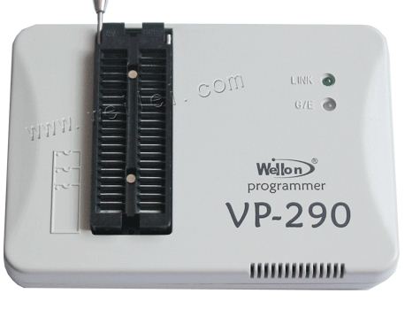
Clearly for these chips to be of any use they need to be programmed. Also
you will need a "GAL Programmer". There are a number of these available on
the web. They are not cheap, typically starting at $200. If you are
doing any serious S100 bus board construction you should get a unit that
programs GAL's, PROMS and EEPROMS. I have been using the
Wellon V290:-
This unit can program almost any type of EPROM or EEPROM out there. However I
found that to program Lattice GAL22V10 (or GAL16V8) one must set the GAL type to
Lattice and set the Erase, Program and Verify options on. Be careful to
match the selected GAL type/manufacture with your actual GAL chip. A wrong
combination will inactivate the GAL immediatly. I used Lattice 22V10 GAL's
from Jameco (#39159).
PALASM
All GAL's (and PAL's) are programmed with a file whose extension is .JED.
There appears to be an earlier version of the .JED file format which programs
like Opel produce. However at least for the Wellon programmer, .JED files
generated by that MSDOS program did not program any of my GAL's correctly.
I wasted a lot of time on this until I found out that the MSDOS program PALASM4
yielded properly programmed 22V10 GAL's.
The MSDOS program PALASM4 is widely available on the web. You can download it
from
here
(or
from the bottom of this page). The program was (and probably still is)
provided by AMD. The manual which they refer to as the MACHXL
Software's user Guide can be obtained
here. As best I can
tell, all the MACHXL menu commands, formats, etc. are identical to the PALASM4
commands. AMD a while back renamed all their PAL and GAL chips MACH1xx, MACH2xx,
MACH3xxx, MACH4xx etc. However the program still recognizes the old PAL
names as well in the program line that specifies the chip type (see below).
I will not describe the PALASM language commands themselves -- they are
very simple and are well described in the manual.
The PALASM download describe above is contained on three 1.44MB floppy disks,
(see bottom of this page for a download).
If you run it on an old PC it should install relatively simply on a hard drive
if you use MSDOS. However it would really be nice to run it on a modern
Windows 7 or 8 (64 bit), or similar system. There are probably a
number of ways to do this, but I really like a Windows program called
DOSBOX which allows you run almost any DOS program in a modern Windows
environment.
DOSBOX is very popular with Gamers and is easy to install. It can
be downloaded from here (or the bottom of
this page).
DOSBOX comes up with Z: as its root directory. Normally you will assign a
folder for your DOS programs. You use the "Mount" command to do this. I
will place it on my F: drive in a new folder in the root directory called
DOSBOX:-
Mount f F:\DOSBOX
Then CD F:
This will bring you to what MSDOS thinks is the root F: drive.
We need
to place the PALASM program with its sub-directories in its own folder,
so make one
MKDIR F:\DOSBOX\PALASM
Download and expand the complete PALASM_C.rar file (see below) to this folder.
There will be a number of sub-folders in this folder.
Before we run PALASM we first need to set a path command for it. DOSBOX
has a special way to implement the MSDOS AUTOEXEC.BAT file when it boots up.
On your windows system its called something like "dosbox-0.74.conf"
and is found at:-
{system drive}:\Users\{username}\AppData\Local\DOSBox\
This is a notepad compatible file, scroll down to the bottom and add:-
[autoexec]
# Lines in this section will be run at startup.
# You can put your MOUNT lines here.
mount F F:\dosbox
REM F:\DOSBOX\PALASM\ PALASM4 Environment Setup
PATH F:\DOSBOX\PALASM\EXE;F:\;"%PATH;C:\DOSBOX\PALASM4\EXE"
SET PALASM=F:\PALASM\
F:
CD F:\PALASM
Save and close the file.
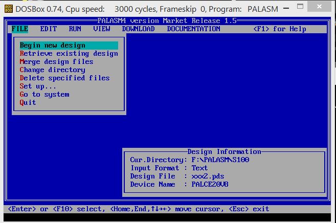
Now when you launch DOSBOX you will end up in the PALASM directory. Type:-
PALASM
It
should look something like this.
The program is fairly straightforward. I keep my S100 bus .PDS and .JED files in a folder
called \PALASM\S100. I actually find it easier to edit a file with windows
Notepad, save
it and then compile it with PALASM rather than use the PALASM editor. You
use the F10 key a lot with this program. The program has an extensive error
checking component. If there is any format error in the starting .PDS file,
errors will be listed and no .JED file will be produced.
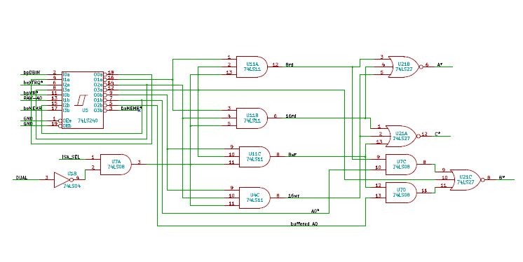
Let us take a simple example of how we can condense a few 74LSxx circuits into a
single GAL.
This is a common circuit we have often used to activate 8 and 16 bit data
buffers for R/W on to the S100 bus. In the case of our ISA to S100 bus
converter board a single GAL can handle the job:-
In fact a few extra functions are also added.
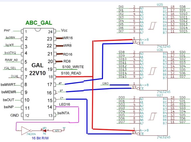
The relevant ABC.PDS file required to generate the ABC.JED file is here:-
TITLE ABC Drivers select signals for U15, U16 & U17 and S100_READ, S100_WRITE
PATTERN
REVISION 0
AUTHOR John Monahan
COMPANY
DATE 03/30/14
CHIP ABC_GAL PALCE22V10 ; Device not selected
;---------------------------------- PIN Declarations ---------------
Pin 1 PHI ;Unused
--- INPUT SIGNALS
Pin 2 bpDBIN ;S100 bus CPU data in
PIN 3 bpWR ;S100 bus CPU data out
PIN 4 bsXTRQ ;LOW if 16 bit request
PIN 5 RAW_A0 ;S100 bus A0
PIN 6 ISA_SEL ;ISA board select
PIN 7 DUAL ;HIGH if two back to back 8 bit writes
PIN 8 bsMWRT ;S100 memory write status
PIN 9 bsMEMR ;S100 memory read status
PIN 10 bsOUT ;S100 I/O write status
PIN 11 bsINP ;S100 I/O read Status
Pin 13 bsINTA ;S100 INTA
PIN 14 LED16 ;Low for S100 16 bit Read/Write
----- OUTPUT SIGNALS
PIN 15 C ;8 bit data TO CPU
PIN 16 B ;data exchange
PIN 17 A ;8 bit data from CPU
PIN 18 S100_READ ;S100 RAM or I/O Read
PIN 19 S100_WRITE ;S100 RAM or I/O Write
PIN 20 RD8 ;(In case needed by DUAL_SEL GAL)
PIN 21 RD16 ;(In case needed by DUAL_SEL GAL)
PIN 22 WR8 ;(In case needed by DUAL_SEL GAL)
PIN 23 WR16 ;(In case needed by DUAL_SEL GAL)
;----------------------------------- Boolean Equation Segment ------
EQUATIONS
RD8 = bpDBIN * bsXTRQ * ISA_SEL * /DUAL
;8 RD
RD16 = bpDBIN * /bsXTRQ * ISA_SEL * /DUAL
;16 RD
WR8 = /bpWR * bsXTRQ * ISA_SEL * /DUAL
;8 WR
WR16 = /bpWR * /bsXTRQ * ISA_SEL * /DUAL
;16 WR
/A = RD8 + RD16 + WR16
/C = RD16 + WR8 + RD8
/B = RD8 * /RAW_A0
+ WR8 * RAW_A0
+ /bsXTRQ
/S100_READ = bsMEMR * /bsINTA
;Read, Set pin 1 direction B <- A
+ bsINP
* /bsINTA
;For now don't allow interrupts
/S100_WRITE = bsMWRT * /bsINTA
+ bsOUT
* /bsINTA
/LED16 = /bsXTRQ * ISA_SEL * /DUAL
What is nice about using these GAL's is that changing the circuit is a trivial
task. The above ABC.PDS file is processed by the PALASM program to yield a
ABC.JED file. This file is then utilized by the Wellon VP-290 program to "burn"
the 22V10 GAL chip.
While the PALASM program also has a "simulator" module to analyze the data, I
find it best to place the chip on a breadboard with a 10 pin dip switch, some
jumpers and a LED bar to confirm what I think I'm getting is in fact what the
GAL delivers. Time spent here will save you much more time later!
One final point about writing PALASM code. You have to be take care to get
active high and active low signals correct. You can either define the pin
signals as active HIGH or active LOW (with a "/" in front of the signal), If you
then have an active LOW in the equations you simply use the name without
the "/". Using a "/" in the equation would be a double negative and flip its
value to HIGH.
Altenatively you can define all pins as HIGH (no "/" anywhere in the pin
definitions part) and then in the equations use a "/" as needed.
The former case actully is more common, though I often use and find the
latter easier to understand.
DOSBOX Download
PALASM Download (DOSBOX version)
(WinRAR format)
PALASM (Main folder (only) as a .ZIP
file)
PALASM Users manual
PALASM Download (MSDOS FLOPPY DISK FORMAT)
see:-
http://www.bitsavers.org/components/mmi/palasm_pleasm/PALASM_4_V1.5/
This page was last modified
on 01/11/2021